Metrology
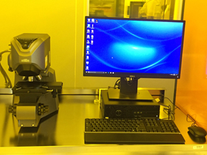
Scanning-Electron Microscope
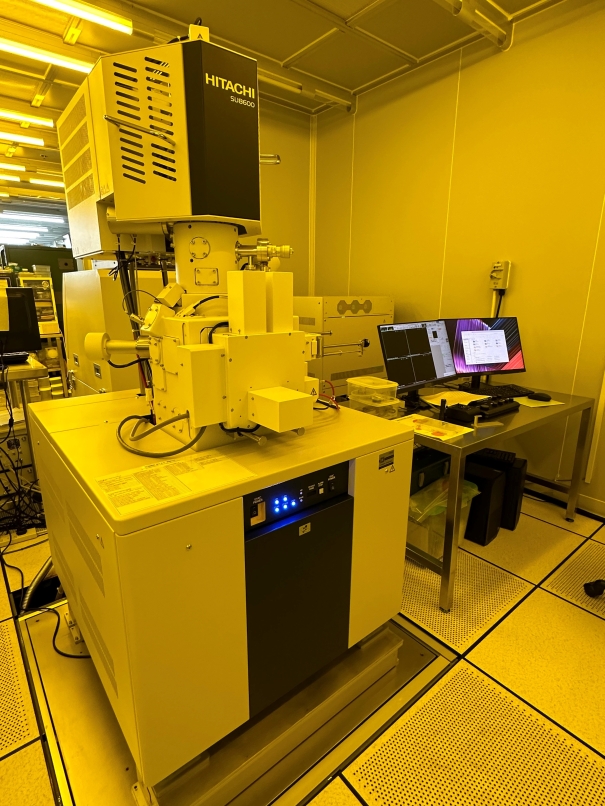
Scanning Electron Microscope HITACHI SU8600
| 1 Resolution | ||
| 0.6 nm (Accelerating voltage 15 kV, WD*1 = 4 mm, Photo magnification x270,000) | ||
| 0.7 nm (Accelerating voltage*2 1 kV, WD*1 = 1.5 mm, Photo magnification x200,000) | ||
| The resolution shall be measured on a resolution measurement specimen (Gold particle on carbon). | ||
| *1 WD (Working Distance) | ||
| *2 Deceleration mode | ||
| 2 Magnification | ||
| High magnification mode | : x100 to x2,000,000 | |
| Low magnification mode | : x20 to x20,000 | |
| NOTE: The magnification range is varied depending on WD and accelerating voltage. | ||
| The magnification is stipulated at 127 mm x 95 mm of display size (Photo magnification). | ||
| 3 Electron optics system | ||
| (1) Accelerating voltage (Vacc) | : 0.50 to 30.00 kV (0.01 kV steps) | |
| (2) Landing voltage (Vland) | : 0.01 to 20.00 kV (0.01 kV steps) | |
| (3) Decelerating voltage | : Maximum -3.50 kV | |
| (4) Detectors | : Scintillator/Photo multiplier detector | |
| Upper detector (BXB filter detector) | ||
| Lower detector (Chamber SE/BSE detectors) | ||
| 4 Specimen Stage | ||
| (1) Drive method | : 5-axis motor drive | |
| (2) Movable range | X-axis 0 to 110 mm | |
| Y-axis 0 to 110 mm | ||
| Z-axis (WB) 1.5 to 40 mm | ||
| R-axis (Rotation) 360° continuous | ||
| T-axis (Tilt) -5° to 70° | ||
| (3) Maximum specimen size | : 100 mm diameter | |
| (4) Maximum specimen height | : 36mm (Including the specimen holder and specimen stub) | |
| (5) Specimen weight | : Air lock method | |
| (6) Specimen exchange | : Control via GUI | |
| (7) Control | : SEM MAP function | |
| Position memory function | ||
| Eccentric rotation function | ||
| Eccentric tilt function [Specimen height: 36 mm * Including the specimen holder] | ||
| Rotation assist function | ||
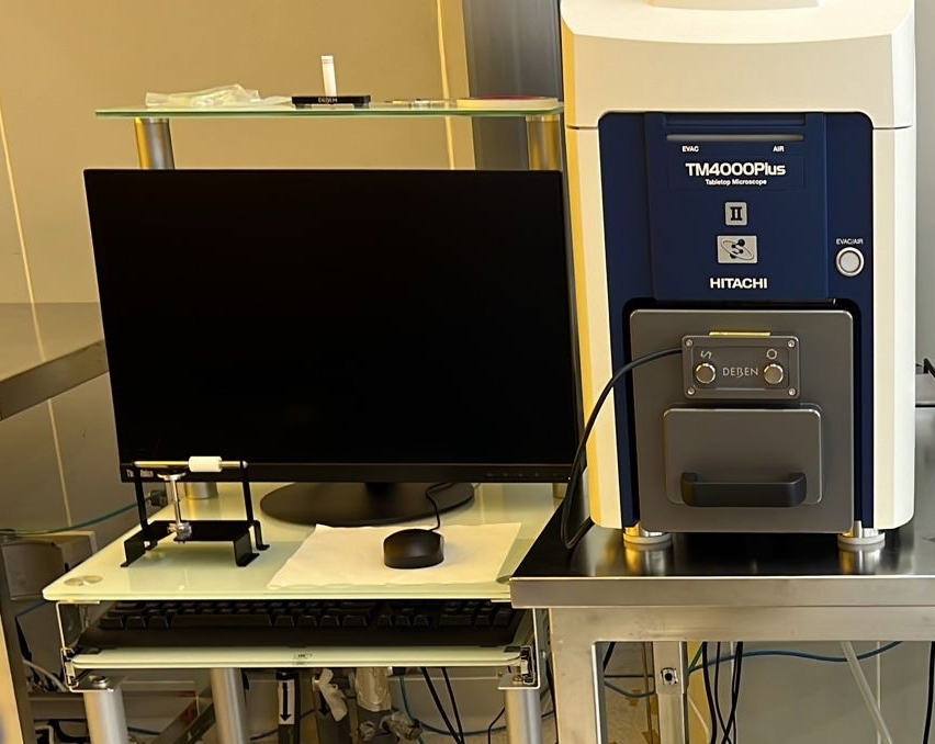
Scanning Electron Microscope HITACHI TM4000Plus
| Magnification | : 10x-100,000x |
| Specimen Stage | : X: 40 mm, Y: 35 mm, Rotation: 0-360 degree |
| Stage Control | : Camera navigation System, 3 axes (X, Y, Rotation) computer controlled |
| Max. Sample Size | : 80 mm (dia.), 50 mm (thickness) |
| Vacuum Mode | : HV, LV |
| Signal Detector | : BSE detector, High-Sensitivity Low- Vacuum SE detector |
| Image Signal | : BSE, SE or Mix (BSE + SE) |
| Image Adjustment | : Auto start, Auto focus, Auto brightness, Camera |
| Image Data Saving | : 2,560 x 1,920, 1,289 x 960, 640 x 480 pixels |
| Image Format | : BMP, TIFF, JPEG |
Film Thickness Measurement
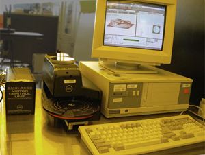
KLA-Tencor P-10 Surface Profiler
Measurement of roughness, waviness, step heights on a surface
| Vertical resolution | : 1 Å (Max. vertical range 13 μm) |
| 25 Å (Max. vertical range 300 μm) | |
| Horizontal resolution | : 0.01 μm at 1 μm/s scan speed |
| Max. Scan length | : 60 mm, 2-D scan only |
| Scan speed | : 1 μm/s to 25 mm/s |
| Stylus force | : 1 - 100 mg |
| Stylus radius | : 12.5 μm |
| Display magnification | : 60 – 240× |
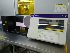
KLA-Tencor P-7 Surface Profiler
Measurement of roughness, waviness, step heights on a surface
| Vertical resolution | : 1 Å (Max. vertical range 13 μm) |
| : 25 Å (Max. vertical range 300 μm) | |
| Horizontal resolution | : 0.025 μm |
| Max. scan length | : 150 mm, 2-D scan only |
| Scan speed | : 2 μm/s to 25 mm/s |
| Stylus force | : 0.5 – 50 mg |
| Stylus radius | : 2 μm |
| Display magnification | : 60 – 240× |
Everbeing SR-4 Resistivity Measurement System
Range from 0.001 to 800k Ohm per square
150 mm probe stand
Keithley 2450 source meter
Tungsten Carbide probe head
| Tip radius | : 40.6 μm |
| Spring Pressure | : 85 grams |
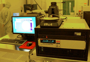
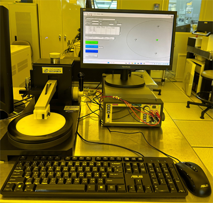
Lucas Pro4-640R Resistivity Measurement System
Range from 0.001 to 800k Ohm per square
150 mm probe stand
Keithley2400 source meter
Tungsten Carbide and Osmium probe heads
| Tip radius | : 40.6 μm |
| Spring Pressure | : 85 grams |
ThetaMetrisis FR-uProbe
| Film thickness measurement | : Silicon Dioxide, Silicon Nitride, Polysilicon, Amorphous Silicon, Positive/Negative Photoresist and etc. |
| Measurable films | : up to 3 layers |
| Standard visible system with Lens in 10x magnification | |
| Measuring light spot size | : 25 μm |
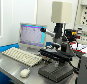
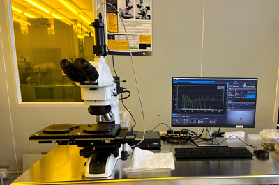
NANOmetrics Nanospec AFT Model 3000
| Single film thickness measurement on silicon substrate: | |
| Silicon Dioxide, Silicon Nitride, Polysilicon, Amorphous Silicon, Positive/Negative Photoresist and etc. | |
| Standard visible system with Lens in 10x magnification | |
| Measuring light spot size | : 25 μm |
J.A. Woollam M-2000VI Spectroscopic Ellipsometer
| Measure the optical constants : refractive Index, extinction coefficients and film Thickness for different materials | |
| Wavelength : 370 nm to 1690 nm, ~ 580 wavelengths | |
| All wavelengths are acquired simultaneously | |
| Focused beam diameter in ~200 μm | |
| Spectral resolution in 1.6 nm, 5 nm bandwidth | |
| Test Base fixed angle of 66°, horizontal sample stage for 100 mm wafer | |
| Automated z-height alignment |
Surface Metrology
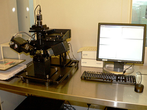
Atomic Force Microscope XE150S (Park XE150S AFM)
- Non-contact AFM imaging to investigate and analyze a sample surface
- Supports up to 6" wafers
- 100 µm × 100 µm XY scan range
- Up to 12 µm Z-scan range
- Radius of the probe tip size: 10 nm
- Enhanced acoustic enclosure
- Fully motorized XY-stage travels the entire 150 mm × 150 mm
Film Stress Measurement System SMSi 3800
- Measure the change of curvature induced in a sample due to the deposited film on a reflected substrate
- Measure 1-D stress and produce a 3-D topographical profile
- For wafer flatness and pattern measurements
- Various stress constants
- Wafer sizes: 2" to 8"
- Thickness limit : less than 11 mm
- Statistical process control and spreadsheet compatibility
- Automatic segmentation calculation
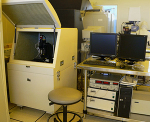
Keyence 3D Laser Confocal Microscope
Keyence VK-X260K 3-D Laser Confocal Microscope provides non-contact, nanometer-level profile, roughness, and film thickness data on any materials
Light sources: 408 nm violet laser source / white-light source
Total magnification: up to 28000×
Optical microscope:
- Pinhole confocal optical system
- Four objectives (10×, 20×, 50× & 150×)
Light-receiving element: 16-bit photomultiplier
Scanning method:
- Automatic upper/lower limit setting
- High-speed light-intensity optimization (AAGII)
- Poor reflected light intensity supplement (Double Scan)
Stages:
- Manual XY-Stage
- 70 mm × 70 mm
- Micrometric motorized Z-translation
Resolution:
- 1 nm lateral resolution
- 0.5 nm Z-axis movement of objective lenses
Observation image:
- Super-high-resolution color CCD images
- 16-bit laser-color confocal images
- Confocal + ND filter optical system
- C-laser differential interference images
Sample size:
- Up to 5"
- Maximum sample height 28 mm
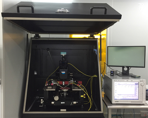
Perfict Lab. Probe Station with Keysight B1500A Analyzer
- Probing stage
- Sample sizes: Up to 152.4 mm (6")
- Probe:
- Probe tip holder: Triaxle cable
- Current leakage: <50 fA
- Probe tip diameter: 20 μm
- Stereo microscope:
- Optical magnification: 20× – 400×
- Keysight B1500A semiconductor device parameter analyzer:
- Current-voltage (IV) measurements with 4 HRSMUs (High-Resolution Source-Monitor Units)
- Current range: ± 100 mA, measuring resolution 1 fA, sourcing resolution 5 fA
- Voltage range: ± 100 V, measuring resolution 0.5 μV, sourcing resolution 25 μV