Sections
Text Area
Thermal Diffusion and Ion-Implantation Module
Implantation
Left Column
Image
Image
Right Column
Text Area
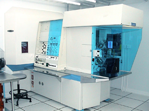
CF-3000 Implanter (Varian CF-3000 Ion Implanter)
| Dose Energy | : 10 to 150 keV |
| Max. Dose (ion/cm2) | : 1015 |
| Processing | Arsenic, Phosphorus, Boron & BF2 implant |
Text Area
Text Area
Oxidator
Left Column
Image
Image
Right Column
Text Area
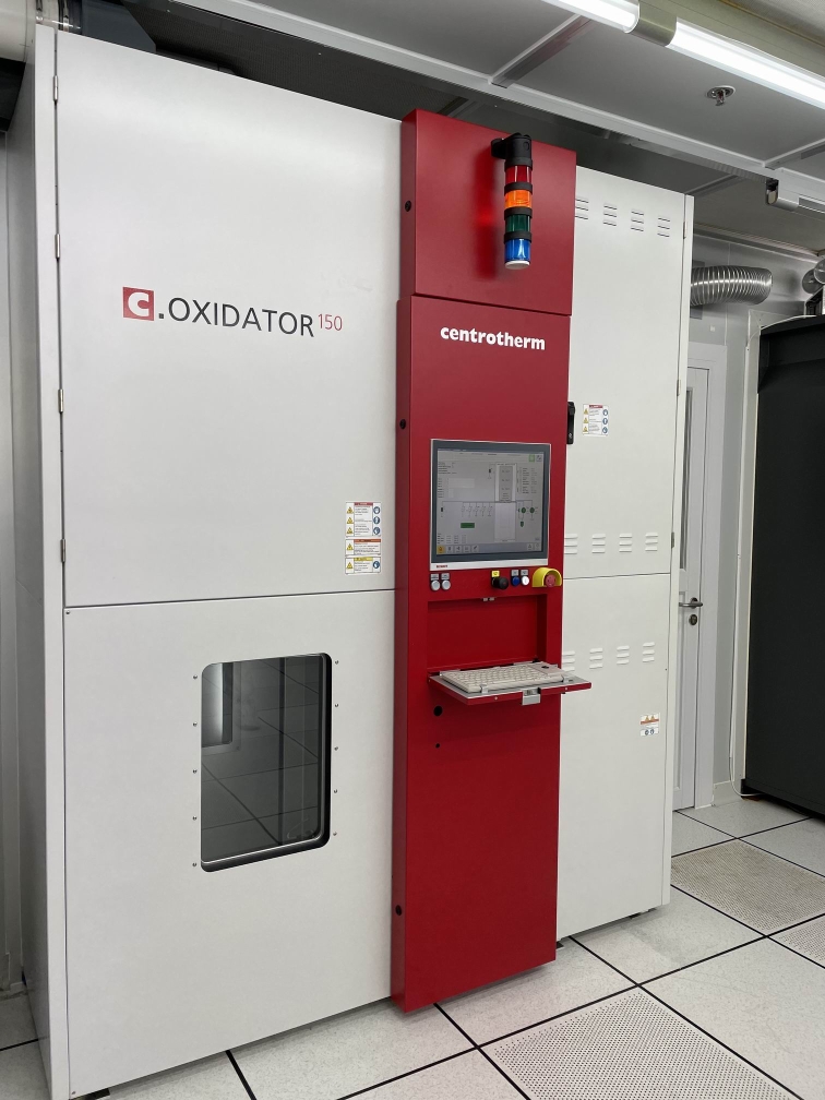
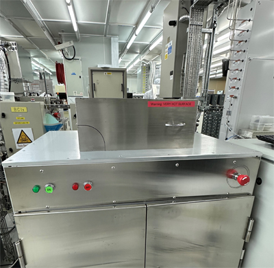
centrotherm SiC Oxidator 150
| Processing | : SiC oxidation and annealing |
| Temperature | : 1350℃ (available gases: Ar, O2, N2, NO, N2O and 5% H2/N2) 1500℃ (available gas: Ar) |
| Substrate sizes | : 4" SiC substrate or small samples |
Text Area
Text Area
CVD
Left Column
Image
Image
Right Column
Text Area
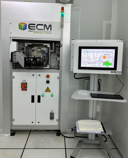
LPCVD HTO
| Processing | : High Temperature Oxide (HTO) |
| Temperature | : 910℃ |
Text Area
Left Column
Image
Image
Right Column
Text Area
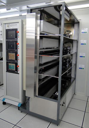
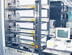
LPCVD
Each deposition has its programmed flow of gas compositions, temperature and pressure
ASM LB45 LPCVD Furnace:
Polysilicon, Amorphous silicon, N-doped Amorphous Silicon, Silicon Germanium, Silicon Nitride,
Low Temperature Oxide (LTO), Phosphorous Silicon Glass (PSG)
Text Area
Left Column
Image
Image
Right Column
Text Area
Diffusion Furnace (ASM Diffusion Furnace)
| Operating temperature | : 400 to 1150 ℃ |
| Processing | : Dry & Wet Oxidation, N/P diffusion, Forming Gas annealing and Drive in |
Text Area
Left Column
Image
Image
Right Column
Text Area
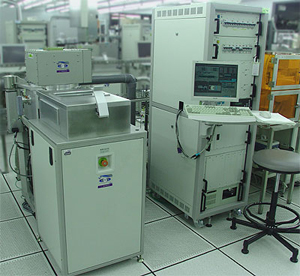
STS PECVD (STS Multiplex PECVD)
Processing:
- Silicon dioxide
- Silicon nitride
- Silicon oxynitride
- Amorphous silicon
Text Area
Left Column
Image
Image
Right Column
Text Area
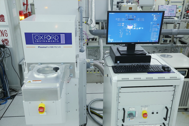
Oxford PECVD
Processing:
- Silicon Dioxide
- Silicon Nitride
- Silicon Oxynitride
- Silicon Dioxide (TEOS)
Text Area
Left Column
Image
Image
Right Column
Text Area
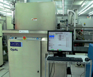
Oxford ALD (Oxford OpAL Plasma ALD)
Thermal and plasma ALD
Processing:
- Aluminum oxide (Al2O3)
- Zirconium oxide (ZrO2)
Text Area
Left Column
Image
Image
Right Column
Text Area
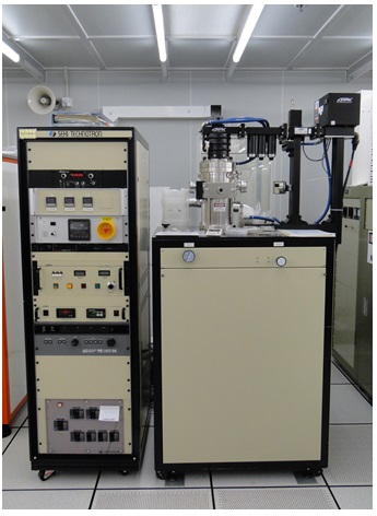
NFF ALD
Thermal ALD
Processing:
- Aluminum oxide (Al2O3)
Text Area
Left Column
Image
Image
Right Column
Text Area
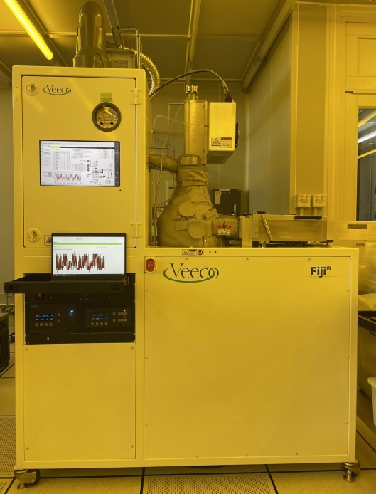
Fiji ALD
Thermal and plasma ALD
Processing:
- Al2O3, AlN, SiO2, Ga2O3, TiO2, TiN
Text Area
Left Column
Image
Image
Right Column
Text Area
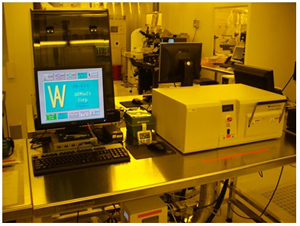
CNT PECVD
| Frequency | : 2455 MHz |
| Processing | : CNT growth |
| Temperature | : 900℃ |
Text Area
Left Column
Image
Image
Right Column
Text Area
RTP-600S (MPT RTP-600S)
| Steady-state temperature stability | : ±2℃ in the range of 250-1150℃ |
| Heating rate | : 0-200℃/sec |
| Cooling rate | : 150℃ max/sec |
| Steady state time | : 1-600 sec |
Text Area
Left Column
Image
Image
Right Column
Text Area
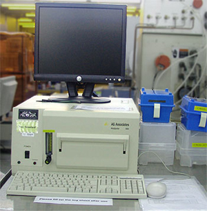
AG610 RTP (Allwin21 AG610 RTP)
- Operating temperature in the range of 400 ℃ to 1000 ℃
- Ion-implantation annealing
- Silicide formation
- Nitridation of thin gates, dielectrics & silicide
- PSG/BPSG reflow
Text Area
Left Column
Image
Image
Right Column
Text Area
AW610 RTP (Allwin21 AW610 RTP)
| Wafer handling | : Manual loading of wafers into the oven, single-wafer processing |
| Wafer sizes | : Small samples and 2", 4" and 6" wafers |
| Ramp-up rate | : Programmable, 10 ℃ to 80 ℃ per second |
| Ramp-down rate | : Programmable, 10 ℃ to 80 ℃ per second |
Operating temperature in the range of 250 ℃ to 800 ℃
Ion-implantation annealing
Silicide formation, nitridation of thin gates, dielectrics & silicide, PSG/BPSG reflow