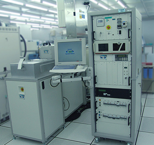
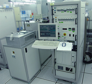
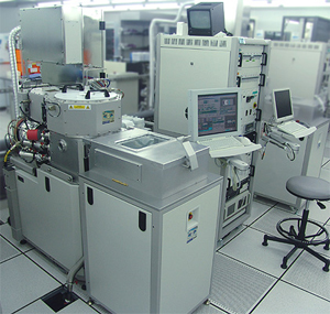
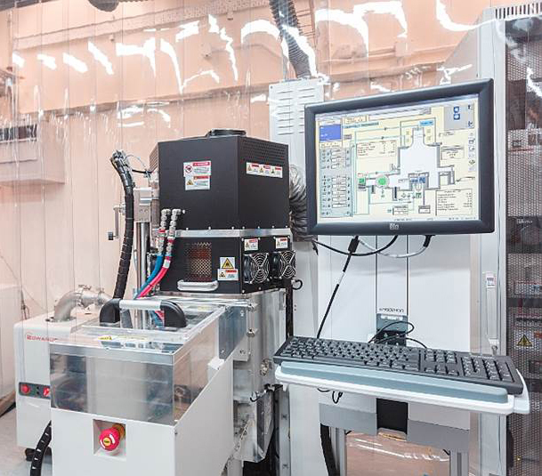
Dry Etching and Sputtering Module
Poly Etcher (STS ICP Poly Etcher)
| Gases available | : HBr, Cl2, O2, N2, He & Ar |
| RF power sources | : 1 × 1000 W (max.) at 13.56 MHz for the coil electrode 1 × 300 W (max.) at 13.56 MHz for the platen electrode |
| Electrode coolant system | : 20℃ |
| High-speed turbo molecular pump | : pumping speed of 1000 L/s at 36000 rpm |
| Fully automatic loadlock transfer system | |
| Substrate size | : 4” single wafers |
Polysilicon etch:
| Minimum line/space | : 0.5 µm |
| Low-Rate polysilicon etch E/R | : ~ 900 Ȧ/min |
| Selectivity to oxide | : 13:1 |
| Selectivity to photoresist | : 12.5:1 |
| Uniformity | : 5% |
Normal-rate polysilicon etch:
| E/R | : >1800 Ȧ/min |
| Selectivity to photoresist | : 2.5:1 |
| Uniformity | : 5% |
GaN Etcher (STS ICP GaN Etcher)
Gases available: BCl3, Cl2, CH4, SF6, O2, He & Ar
RF power sources:
1 × 1000 W (max.) at 13.56 MHz for the coil electrode
1 × 300 W (max.) at 13.56 MHz for the platen electrode
Electrode coolant system: 5 to 30 oC
High-speed turbo molecular pump: pumping speed of 1000 L/s at 36000 rpm
Fully automatic loadlock transfer system
Substrate sizes: 2", 4" or 6” single wafers or specimens
GaN etch:
E/R: ~5000 Ȧ/min
Selectivity to oxide: 10:1
Sapphire etch:
E/R: ~700 Ȧ/min
Selectivity to oxide: 1.5:1
DRIE Etcher #1 (STS ICP DRIE Etcher)
Gases available: C4F8, SF6, O2, N2, He & Ar
RF power sources:
1 × 1000 W (max.) at 13.56 MHz for the coil electrode
1 × 300 W (max.) at 13.56 MHz for the platen electrode
Electrode coolant system: 5 to 30 oC
High-speed turbo molecular pump: pumping speed of 1000 L/s at 36000 rpm
Fully automatic loadlock transfer system
Substrate size: 4" wafers
Silicon etch:
Minimum line/space: 0.5 µm
Low-rate silicon etch E/R: from 500 Ȧ/cycle
Normal-rate silicon etch E/R: up to 2 µm/min
Selectivity to photoresist: > 50:1
Selectivity to oxide: > 80:1
Uniformity: 7%
DRIE Etcher #2 (STS ICP DRIE Etcher)
Gases available: C4F8, SF6, O2, N2, He & Ar
RF power sources:
1 × 3600 W (max.) at 13.56 MHz for the primary source
1 × 3000 W (max.) at 13.56 MHz for the secondary source
1 × 200 W (max.) at 13.56 MHz for the platen electrode
1 × 200 W (max.) at 300 - 500 kHz for the platen electrode
Electrode coolant system: 20 to 40 oC
High-speed turbo molecular pump: pumping speed of 2350 L/s at 25000 rpm
Fully automatic loadlock transfer system
Substrate size: 4" wafers
Silicon etch:
Minimum line/space: 0.5 µm
Aspect ratio: up to 60:1
Low-rate silicon etch E/R: From 0.7 µm/min (700 Ȧ/Loop)
Normal-rate silicon etch E/R: 2 µm/min
Fast-rate silicon etch E/R: 18 µm/min
Selectivity to photoresist: from 12:1 to 250:1
Selectivity to oxide: from 24:1 to 500:1
Uniformity: < 5%
DRIE Etcher #3 (SPTS Rapier DRIE Etcher)
Gases available: C4F8, SF6, O2, N2, He & Ar
RF power sources:
1 × 1000 W (max.) at 13.56 MHz for the coil electrode
1 × 300 W (max.) at 13.56 MHz for the platen electrode
Electrode coolant system: 20 oC
High-speed turbo molecular pump: pumping speed of 1000 L/s at 36000 rpm
Fully automatic loadlock transfer system
Substrate size: 4" wafers
Silicon etch:
Minimum line/space: 1 µm
Low-rate silicon etch E/R: 1 µm/min
Normal-rate silicon etch E/R: up to 2 µm/min
Selectivity to photoresist: > 50:1
Selectivity to oxide: > 100:1
Uniformity: 7%
AOE Etcher (STS ICP AOE Etcher)
Gases available: C4F8, CF4, CHF3, O2, N2, H2, He & Ar
RF power sources: 1× 3000 W (max.) at 13.56 MHz for the coil electrode, 1× 600 W (max.) at 13.56 MHz for the platen electrode
Electrode coolant system: -5 to 30 oC
High-speed turbo molecular pump: pumping speed of 2000 L/s at 48000 rpm
Fully automatic loadlock transfer system
Substrate size: 4" single silicon or quartz wafer
Silicon oxide etch
Minimum Line/Space: 0.5 µm
Silicon oxide etch E/R: > 2500 Ȧ/min
Selectivity to photoresist: > 4:1
Selectivity to polysilicon: > 15:1
Uniformity: 7.5%
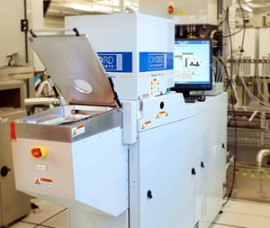
Oxford Oxide Etcher
Gases available: C4F8, CF4, CHF3, SF6, H2, O2, He, Ar, N2
RF power:
1 x 3000W(max) at 13.56MHz for coil electrode
1 x 600W(max) at 13.56MHz for platen electrode
Electrode coolant system: 5 to 60℃
High speed turbo molecular pump: pumping speed of 1280 L/s at 39000 rpm
Fully automatic loadlock transfer system
Substrate size: 4" or 6" single full wafer
Silicon Dioxide Etch (C4F8/H2/He)
E/R: ~ 2000 Ȧ/min (PR mask)
E/R: ~ 3500 Ȧ/min (Poly-Si mask)
Selectivity to Photoresist: ~ 4:1
Selectivity to Poly-Silicon: ~ 8:1
Silicon Nitride Etch (C4F8/H2/He):
E/R: ~ 3000 Ȧ/min (PR mask)
Selectivity to Photoresist: ~ 6:1
Silicon Etch (SF6/C4F8):
E/R: ~ 3500 Ȧ/min (SiO2 mask)
Selectivity to Photoresist: ~ 8:1
Remark: Accept Cr mask; not for etching metals.
IPC 3000 Asher #1, #2 and #4 (Branson IPC 3000 Asher)
Gases available: O2 & N2
Microwave power: 400 W (max.) at 13.56 MHz
Substrate sizes: 2", 4" and 6" wafers or specimens
IPC 3000 Asher #3 (Branson IPC 3000 Asher)
Gases available: O2 & N2
RF power: 400 W (max.) at 13.56 MHz
Substrate sizes: 2", 4" and 6" wafers or specimens
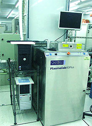
Oxford RIE Etcher (Oxford 80 Plus RIE Etcher)
Gases available: CHF3, SF6, O2, CF4, Ar, N2, He & H2
RF power: 500 W at 13.56 MHz
Huber electrode coolant system: -40 to 200 oC
Substrate sizes: 4" wafers, up to 3 wafers per run or specimen
Silicon dioxide etch:
E/R: ~363 Ȧ/min for LTO
E/R: ~352 Ȧ/min for thermal oxide
Selectivity to photoresist: 2.6:1
Selectivity to silicon nitride: 0.8:1
Selectivity to silicon: 6.7:1
Uniformity: 3.6%
Silicon nitride etch:
E/R: ~810 Ȧ/min
Selectivity to photoresist: 1.5:1
Selectivity to silicon dioxide: 2.1:1
Selectivity to silicon: 5.4:1
Uniformity: 5.8%
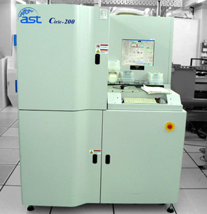
AST Metal Etcher (AST Cirie-200 Metal etcher)
Chlorine & fluorine-based barrel-type system for etching aluminum
Gases available: Cl2, BCl3, CF4, CHF3, He, Ar, O2 & N2
RF power: 1000 W (max.) at 13.56 MHz
Bias power: 1000 W (max.) at 13.56 MHz
Substrate size: 4" wafers
Aluminum Etch
Al etch rate: 1700 Ȧ/min
PR etch rate: 1000 Ȧ/min
SiOx etch rate: 300 Ȧ/min
Memsstar XeF2 Silicon Etcher
Gases available: XeF2
Substrate size: 2", 4" single wafer or specimens
Silicon or Germanium Etch
Mask used: Photoresist, Oxide or Si3N4
Etch rate with bright field mask: ~900 Ȧ/min
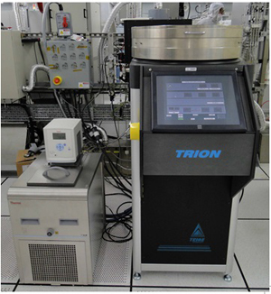
Trion RIE Etcher (Trion Phantom III RIE etcher)
Gases available: CHF3, SF6, O2, CF4, Ar, N2, He & H2
ICP power: 600 W (max.) at 13.56 MHz
RF power: 600 W (max.) at 13.56 MHz
Electrode coolant system: 0 to 30 oC
Substrate sizes: 4" wafers, up to 3 wafers per run or specimens
Silicon dioxide etch: ~500 Ȧ/min
Silicon nitride etch: ~850 Ȧ/min
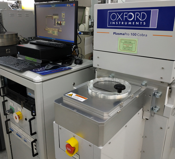
Oxford Aluminum Etcher (Oxford Cobra 100 Aluminum Etcher)
Gases available: Cl2, BCl3, HBr, CF4, SF6, O2 and Ar
RF power sources:
1 × 3000 W (max.) at 13.56 MHz for the coil electrode
1 × 300 W (max.) at 13.56 MHz for the platen electrode
Electrode coolant system: 5 to 60 oC
High-speed turbo molecular pump: pumping speed of 1250 L/s at 37800 rpm
Fully automatic loadlock transfer system
Substrate size: 4" wafers
Aluminum/Aluminum-Si etch:
Minimum line/space: 0.5 µm
High-rate aluminum etch E/R: 3000 Ȧ/min
Normal-rate aluminum etch E/R: 1800 Ȧ/min
Selectivity to photoresist: > 2:1
Selectivity to oxide: > 10:1
Uniformity: 5% (etch from edge to center)
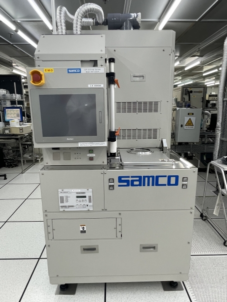
Samco ICP Metal Etcher
Remark:
1. For Non-standard process, please contact NFF (CWB) technicians.
2. Etch materials: Metal and metal compounds only.
Gases available: BCl3, Cl2, O2, He, Ar, CHF3, CF4 and SF6
RF power source:
1 x 1000W (max) at 13.56MHz for coil electrode
1 x 300W (max) at 13.56MHz for platen electrode
Electrode coolant system: 20℃
High speed turbo molecular pump: pumping speed of 1300 L/s at 560 Hz
Fully automatic loadlock transfer system
Substrate size: 2", 4" single wafer or specimens
NFF RIE Etcher
Gases available: CF4, CHF3, SF6 and O2
RF power: 120 W
Chiller temperature: 20 oC
Fully automatic loadlock transfer system
Substrate size: 4" wafers
Nitride etch rate: ~500 Ȧ/min
Oxide etch rate: ~460 Ȧ/min
Si etch rate: ~50 to 470 Ȧ/min
Photoresist etch rate: ~151 to 400 Ȧ/min
Oxford GaN-InP Etcher
Gases available: Cl2, BCl3, CH4, H2, N2, SF6, O2, He and Ar
RF power source:
1 x 3000W (max) at 13.56MHz for coil electrode
1 x 600W (max) at 13.56MHz for platen electrode
Electrode coolant system: -10 to 200℃
High speed turbo molecular pump: pumping speed of 1280 L/s at 39000 rpm
Fully automatic loadlock transfer system
Substrate sizes: 2", 4" or 6" single full wafer
GaN Etch:
E/R: ~6000 Ȧ/min
Selectivity to Oxide: 9:1
InP Etch
E/R: ~6000 Ȧ/min
Selectivity to Oxide: 10:1
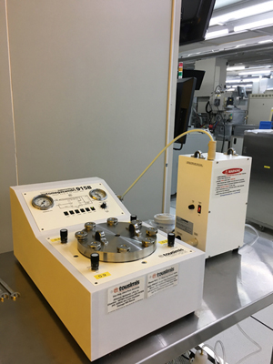
Critical Point Dryer
Tousmis Automegasamdri®-915B, Series-B Critical Point Dryer
- Automatic supercritical point dryer
- All internal surfaces are inert to CO2 and ultra-pure alcohols.
- 0.08 µm internal filtration system delivers clean filtered LCO2 to the process chamber.
- Small samples and up to 6" wafers
- Up to five wafers per single process
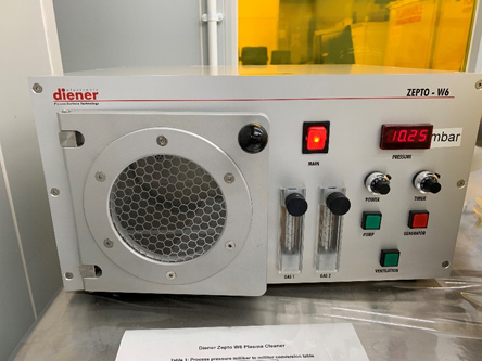
Diener Plasma Cleaner
Gases available: air
RF power source: 50 W (max) at 13.56 MHz
Substrate size: 2", 4" or specimens
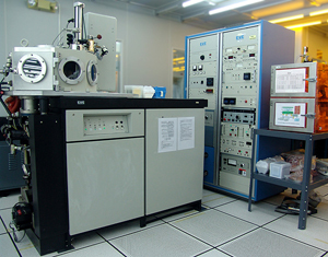
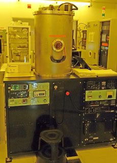
Varian 3180 Sputterer
Gases available: Ar & N2
DC sputtering power: 3 × 12 kW
RF back-sputtering power: 600 W at 13.56 MHz
Fully automatic wafer-handling system
Substrate size: 4" wafers
Chamber pressure: 5 × 10⁻⁷ torr
Targets available: Mo, Pure Al, Al-Si & Ti
Sputtering rate (Ȧ/sec):
~160 Ȧ/sec for pure Al
~180 Ȧ/sec for Al/Si (1%)
~40 Ȧ/sec for Ti
~160 Ȧ/sec for Mo
No photoresist on wafers is allowed.
CVC-601 Sputterer
Gases available: Ar & N2
DC sputtering power: 1 × 3 kW
RF sputtering power: 1200 W at 13.56 MHz
Chamber pressure: 5 × 10⁻⁷ torr
Substrate sizes: 2", 4" & 6" wafers or 4" square glass substrates
Targets available: Cu, TiW & Au
Targets available on request: Ti, Cr & Al-Si
Sputtering rate (Ȧ/min):
~500 Ȧ/min for Al-Si
~175 Ȧ/min for TiW
~160 Ȧ/min for Au
~1,000 Ȧ/min for Cu
No photoresist on wafers is allowed.
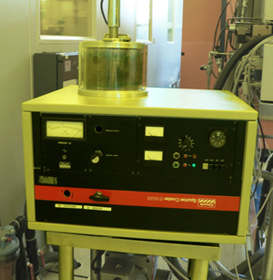
ARC-12M Sputterer
Gases available: Ar, O2 & N2
DC sputtering power: 2 × 250 W
RF sputtering power: 600 W at 13.56 MHz
Chamber pressure: 1.5 x 10⁻⁵ torr
Substrate sizes: 2", 4" wafer or square glass, or specimens
Targets available: Ag, Al, Al/Si (1%), Au, Cu, Cr, Hf, Mo, Pt, Ti, TiW, Ni
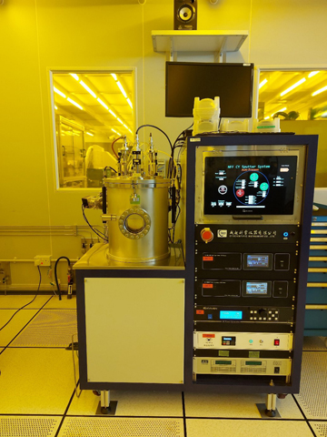
NFF-CY1 Sputterer
Gases available: Ar, O2 & N2
DC sputtering power: 1 x 100W
RF sputtering power: 1 x 100W
Chamber pressure: 5 x 10⁻⁶ torr
Substrate sizes: 2", 4" wafer or square glass, or specimens
Targets available: Al, Ti, Cr, Al-Si, Ni, Mo, dielectric targets (such as TiN, TaN)
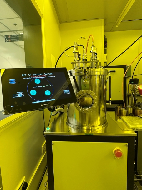
NFF-CY2 Sputterer
Gases available: Ar, O2 & N2
DC sputtering power: 1 x 100W
RF sputtering power source: 2 x 100W
Chamber pressure: 5 x 10⁻⁶ torr
Substrate sizes: 2", 4" wafer or square glass, or specimens
Targets available: Al, Ti, Cr, Al-Si, Ni, Mo, dielectric targets (such as TiN, TaN), Cu, Ag, Au
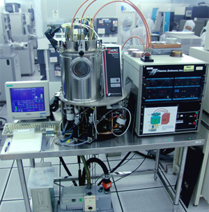
Cooke Evaporator #2 (Cooke E-Beam Evaporator)
Gases available: N2
E-beam power: 1 × 3 kW
Chamber pressure: 8 × 10⁻⁷ torr
Substrate sizes: 2" or 4" wafers
Sources available (in Phase III (EC)): Al, Ni, Ti, Au, Cr, Pt, Fe, SiO2, Ag
No photoresist on wafers is allowed for the Cook Evaporation System.
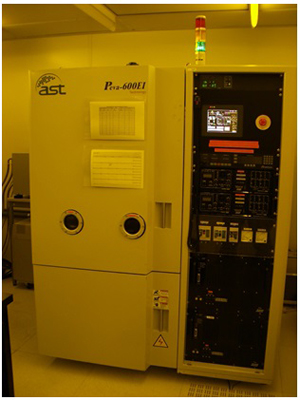
AST 600EI Evaporator (AST Pava-600EI E-Beam Evaporator)
Gases available: O2 and N2
E-beam power: 2 × 6 kW
Chamber pressure: 9 × 10⁻⁸ torr
Substrate sizes: 2" and 4" wafers or specimens
Sources available: Al, Au, Ti, Ni, Cr, Ge, Pt, Ag, ITO
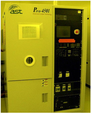
AST 450I Evaporator (AST Pava-450I E-Beam Evaporator)
Gases available: N2
E-beam power: 1 × 3 kW
Chamber pressure: 9 × 10⁻⁸ torr
Substrate sizes: 2” wafer or specimens
Sources available: Al, Ti, Au & Ni
Edward Sputterer (Au) for SEM
Gases available: Ar
RF power: 100 W at 13.56 MHz
Chamber pressure: 1 × 10⁻³ torr
Substrate sizes: 2" and 4" wafers or square glasses, or specimens
Targets available: Au (For SEM only)