Sections
Text Area
Wet Etching and CMP Module
Wet Station
Left Column
Image
Image
Right Column
Text Area
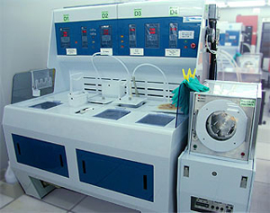
Wet Stations A, B, C, D, E, F, G and H
Wet processing:
- Silicon Etch using KOH / TMAH (25%)
- Photoresist Strip / ITO Etch
- Aluminum Etch / Pad Oxide Etch
- Oxide / Nitride Etch
- Wafer Cleaning (RCA)
- Wafer Cleaning (Piranha Clean)
- Solvent Cleaning
Text Area
Left Column
Image
Image
Right Column
Text Area
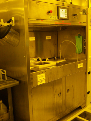
Wet Station M
- MS2001 resist stripper
- FHD5 manual developer
- Quick dump rinsers
- Small samples of sizes of up to 6"
Text Area
Left Column
Image
Image
Right Column
Text Area
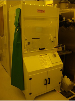
Wet Station O
- Hydrochloric acid etch prior to E-Beam metallization
- DI water gun for rinsing
- N2 gun for drying
- Small samples of sizes of up to 6"
Text Area
Left Column
Image
Image
Right Column
Text Area
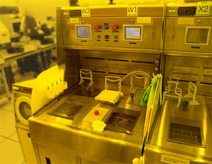
Wet Stations W, X, Y and Z
- MS2001 resist stripper
- FHD5 manual developer
- Quick dump rinsers
- Small samples of sizes of up to 6"
Text Area
Text Area
CMP
Left Column
Image
Image
Right Column
Text Area
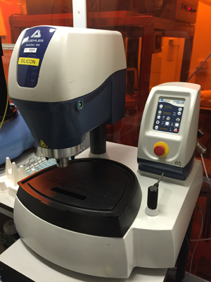
Buehler Polisher #1
- Polished for silicon, silicon oxide or silicon nitride
- > 5 mm2 to 4" wafer size
- 100 - 800 µm wafer thickness
Text Area
Left Column
Image
Image
Right Column
Text Area
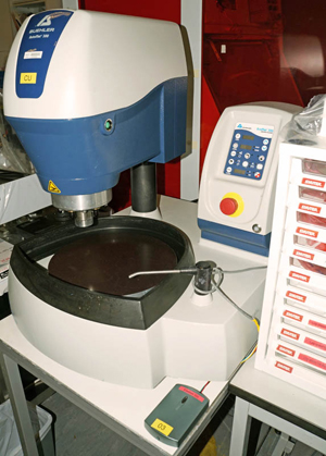
Buehler Polisher #2
- Polished for copper, CNT, silicon, silicon oxide or silicon nitride
- > 5 mm2 to 4" wafer size
- 100 - 800 µm wafer thickness
Text Area
Left Column
Image
Image
Right Column
Text Area
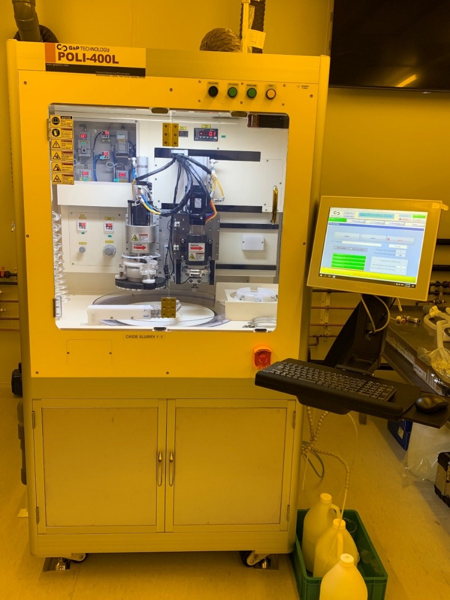
GnP CMP
| Equipment model | : POLI-400L |
| Polishing materials | : Silicon dioxide or Polysilicon |
| Sample Size | : 1"x1" or 4" |
| Wafer Thickness | : 400-550 µm |
| Wafer Carrier | : Membrane style with floating ring |
| Polishing platen and wafer carrier speed range |
: 30-200 rpm Oscillating Arm Pad Conditioning |
Text Area
Text Area
Electroplating
Left Column
Image
Image
Right Column
Text Area
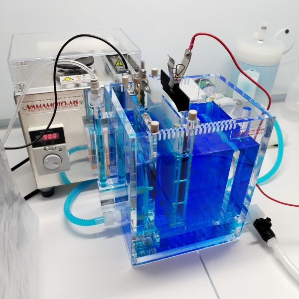
Copper Electroplating
| Plating metal | : Copper |
| Substrate size |
: 4-inch wafer or coupon (<50mm length) attached on metallized 4-inch wafer (seed layer covering the whole wafer to the edge is needed.) |
| Wafer Thickness | : Standard 525 micron |