Sections
Text Area
Mask-Making Module
Mask Writing System
Left Column
Image
Image
Right Column
Text Area
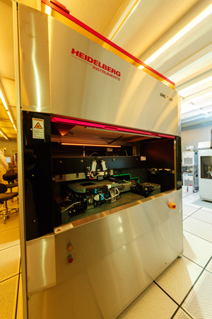
Heidelberg DWL 2000 Laser Lithography System
With an Environment Chamber (providing a stable environment for the system)
- Laminar airflow (adjustable): 0.3 – 0.5 m/s
- Temperature stability: ± 0.1 °C
- Air quality: Class 10
Stage System (with linear motors, air bearings and interferometric position control)
- Maximum substrate size: 9" × 9"
- Maximum write area: 200 × 200 mm² (min. 5 mm from the substrate edge)
- Substrate thickness: 0 to 7 mm
Writing Performance
- Write modes: I and II
- Minimum feature sizes: 0.5 µm, 0.7 µm
- Edge roughness (3σ): 40 nm, 50 nm
- CD uniformity (3σ): 60 nm, 80 nm
- Alignment measurement accuracy (3σ): 60 nm, 70 nm
- Overlay accuracy (3σ): 160 nm, 200 nm
- Write speed (mm2/minute): 29, 110
Left Column
Image
Image
Right Column
Text Area
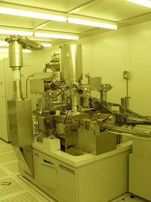
JEOL JBX-6300FS E-Beam Lithography System
Writing Mode: High-speed or high-precision
Beam Current: 30 pA to 20 nA
Scanning Speed: 12M to 250 Hz
Accelerate Voltage: 20, 50 or 100 kV
Max. Field Sizes (µm2): High-speed mode: 2000 (20 kV), 1000 (50 kV) or 500 (100 kV); High-Precision Mode: 250 (20kV), 125 (50kV) or 62.5 (100kV)
Mask: 5" × 5" × 0.09"
Wafers: 4" or 2"
Nanoimprint Mask: 65 mm × 65 mm × 6.35 mm
Chip Samples: 2 cm × 2 cm, 1.5 cm × 1.5 cm or 1 cm × 1 cm
Text Area
Scanning-Electron Microscope