Sections
Text Area
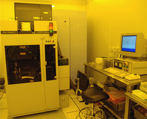
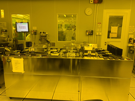
Photolithography Module
Stepper, Aligner and Bonder
Left Column
Image
Image
Right Column
Text Area
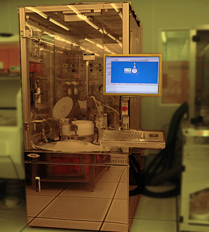
Nanoscribe 3-D Printer
Resolution (depends on the objective lens and the resist):
- 3-D lateral feature size: ≤ 200 nm
- 2-D lateral resolution: ≤ 500 nm;
- Vertical resolution: ≤ 1,500 nm
Speed:
- Beam-scanning speed: 10 mm/s
- Piezo-scanning speed: 100 µm/s
Range:
- Motorized xy-scanning stage range: 100 × 100 mm²
- x-y-z piezo range: 300 x 300 x 300 µm³
- x-y galvo-scan range: 200 - 600 µm Ø depends on scanning objective
Maximum structure height:
- IP-Q 10x lens DiLL: 8 mm
- IP-S 25x lens DiLL: 3 mm
- IP DiP 63x lens DiLL: 3 mm
- Oil immersion with 170 µm glass: 150 µm
Minimum feature size
- 10x lens: ~2 µm x, y and ~10 µm z
- 25x lens: 0.6 µm x, y and ~3.3 µm z
- 63x lens: 150 nm x, y and 800 nm z
Objective:
- Immersion Objective: 63×, NA = 1.4; WD = 190 µm,
for high-resolution structures, printing field (Galvo Ø) = 200 um;
Typical slicing distance = 0.3 µm; Typical hatching distance=0.2 µm - Immersion Objective: 25×; NA = 0.8; WD = 380 µm,
for mesoscale structures; Printing field (Gavle Ø) = 400 µm;
Typical slicing distance =1 µm; Typical hatching distance=0.5 µm - Air Objective: 20×, NA = 0.5; WD = 2100 µm,
or 2D maskless lithography; Printing field (Galvo Ø) = 600 µm;
Typical slicing distance=3-6 µm; Typical hatching distance= 0.7-1.2 µm - Immersion Objective: 10x, NA=0.3; WD=700 um,
for rapid prototyping; Printing field (Galvo Ø) =1000 µm;
Typical slicing distance= 5 µm; Typical hatching distance =1 µm
Sample holders:
| Model | Substrate Type | Substrate Dimensions | Substrate Thickness |
| DiLL | DiLL substrate | 25 mm × 25 mm | 0.7 mm |
| Microscope slide | 24 – 26 mm × 50 – 76 mm | 1.0 mm | |
| Borosilicate | Ø 30 mm | 0.17 mm | |
| Cover slip | Ø 25.4 mm | 0.3 mm | |
| Multi-DiLL | DiLL substrate | 25 mm x 25 mm | 0.5 mm |
| 2" wafer | wafer | Ø 2" | 0.35 - 0.55 mm |
| 4" wafer | wafer | Ø 4" | 0.35 - 0.55 mm |
| 10 × Ø 30 mm | Cover slip | Ø 30 mm | 0.17 mm |
Printing configuration:
| Configuration | Objective | Immersion medium | Substrate(s) | Resist |
| Oil immersion | 63× NA 1.4 | oil | glass 170 µm | IP-L 780 |
| Air | 20× NA 0.5 | air | Silicon, glass | AZ resist, SU8 |
|
Dip-in Laser Lithography |
10x NA 0.3 | silicon | IP-Q | |
| 25× NA 0.8 | ITO-coated glass, Silicon | IP-S | ||
| 63× NA 1.4 | fused silica | IP-DIP |
Text Area
Left Column
Image
Image
Right Column
Text Area
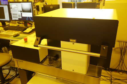
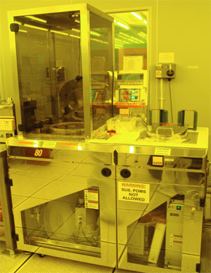
ASML Stepper
| Light-source illumination | : i-line (365 nm) |
| Resolution | : 0.5 µm |
| Overlay alignment accuracy | : ± 0.1µm (3 σ) |
| Wafer sizes | : 4" or 6" |
| Field sizes | : 15 mm × 15 mm or 10 mm × 10 mm (on wafer) |
| Reduction ratio | : 5:1 |
| Photomask size | : 5" square |
Text Area
Left Column
Image
Image
Right Column
Text Area
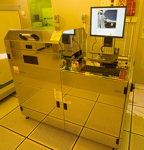
Karl Suss Bonder XB8
Adhesive, Anodic, Eutectic bonding and Silicon fusion prebonding
| Wafer size | : > 2 cm x 2 cm, 4", 6" & 8" |
| Substrate material | : Silicon or Pyrex Glass |
| Pressure | : 1x10e-5 mbar to 3 bars |
| Bonding force | : 3500 N ~ 100K N (8") |
| Temperature | : RT to 500 ℃ |
| Controllable Voltage range | : 0 – 2000 V |
| Controllable Current range | : 0-15 mA |
Text Area
Left Column
Image
Image
Right Column
Text Area
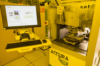
SET ACCµRA100 Flip-Chip Bonder
Flip-chip/Die bonding
| Substrate size | : 1 mm x 1 mm to 100 mm x 100 mm |
| Chip size | : 1 mm x 1 mm to 50 mm x 50 mm |
| Post-bonding accuracy | : ± 0.5 µm |
| Bonding force | : 3500 N ~ 100K N (8") |
| Bonding force | : 1 N to 1000 N |
| Temperature | : RT to 400℃ |
Text Area
Left Column
Image
Image
Right Column
Text Area
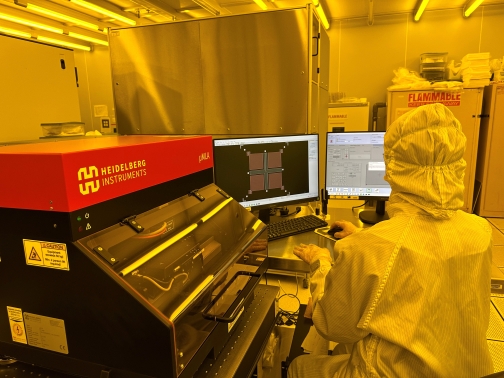
Heidelberg Maskless Aligner µMLA
| Light sources UV LED | : i-line (365 nm) |
| Minimum feature size | : 0.8 µm |
| Alignment accuracy | : ≤ 1 µm |
| Substrate size | : 10 x 10mm² to 5" x 5" |
| Substrate thickness | : standard wafer and photomask |
| Allowed Photoresist | : AZ1505, AZ703 and AZ7908 only |
Text Area
Left Column
Image
Image
Right Column
Text Area
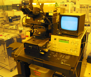
Karl Suss MA6 #1 and #2
| Light-source illumination | : i-line (365 nm) |
| Resolution | : 1 µm |
| Substrate sizes | : > 5 mm² to 2" or 4" |
| Photomask size | : 5” square |
| Exposure modes | : Contact (soft, hard, low vacuum and Vacuum) Proximity (exposure gap 1-300 µm); Flood Exposures |
| Alignment methods | : Top-Side Alignment (TSA); Bottom-Side Alignment (BSA) |
| Alignment accuracy | : TSA (down to 0.5 µm); BSA (down to 1 µm) |
| No. of machines installed | : 2 |
Text Area
Left Column
Image
Image
Right Column
Text Area
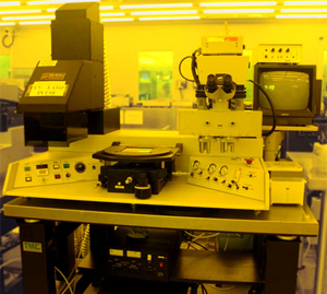
AB-M Aligner #1 (UV)/(DUV) and #2 (UV)
| Light-source illumination | : DUV/UV wavelength selectable (500 W Mercury DUV lamp) |
| Alignment printing mode | : Manual |
| Soft contact | : Contact vacuum adjustable |
| Hard contact | : Full vacuum contact |
| Photomasks | : 5" square or 7" square |
| Substrate sizes | : > 5 mm² to 4" square, or 6" |
| Special feature | : Backside alignment using infrared |
| No. of machines installed | : 2 |
Text Area
Left Column
Image
Image
Right Column
Text Area
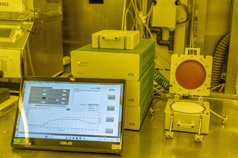
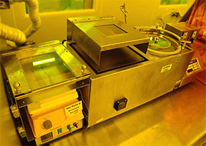
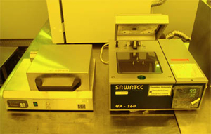
NILT Nanoimprint
| Thermal NIL | : emperature up to 250 ℃ |
| UV NIL | : @365nm (with temperature up to 200 ℃) |
| Imprint in Vacuum | : ~80 mbar |
| Imprint stack thickness | : Up to 2 mm |
| Replicable structures | : ~40 nm up to 100 µm |
| Imprint Pressure | : Up to 5 bar |
Text Area
Left Column
Image
Image
Right Column
Text Area
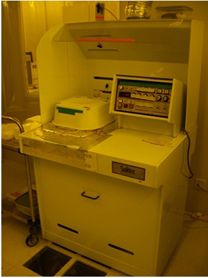
SVG88 Coater Track and SVG88 Developer Track
Automatic tracks for resist coating and developing
| No. of tracks | : 2 |
| Coat track feature | : Vapor prime Chill plate |
| : Coat module Backside rinse |
|
| : Frontside edge-bead remover 2 hot plate ovens |
|
| Develop track | : Developer module, chill plate, 2 hot plate ovens |
| Coating uniformity | : ± 0.3 % |
| Wafer size | : 4" and 6" |
| Wafer loading/unloading | : Cassette to cassette |
Text Area
Left Column
Image
Image
Right Column
Text Area
EVG Spray Coater
| Speed range | : up to 10,000 rpm |
| Ramp-up speed | : 0-40,000 rpm/s |
| Heat-chuck temperature | : up to 70 ± 1 ℃ |
| Spray speed integrate with heat chuck | : < 1,500 rpm |
| Spray-coating nozzle | : Ultrasonic Atomizer Nozzle |
| Syringe dispense rate | : 0.01 ml/s to 5 ml/s |
| Substrate sizes | : up to 200 mm or 150 mm × 150 mm |
Text Area
Left Column
Image
Image
Right Column
Text Area
SUSS Coater
| Spin-speed range | : 0 to 7000 rpm |
| Spin-speed acceleration | : 0 – 5000 rpm/s |
| Coat system | : Open Bowl; GYRSET |
| Substrate sizes | : > 5 mm² to 6" or 5" square for single-side coating, 4" for double-side coating |
| Others | : Programmable bowl auto-clean; Edge-bead remover |
Text Area
Left Column
Image
Image
Right Column
Text Area
CEE Coater
| Spin-speed range | : 0- 6,000 rpm |
| Spin-speed acceleration | : 0-30,000 rpm/s |
| Substrate sizes | : 4" or 6" |
| Others | : Frontside-edge bead remove |
Text Area
Left Column
Image
Image
Right Column
Text Area
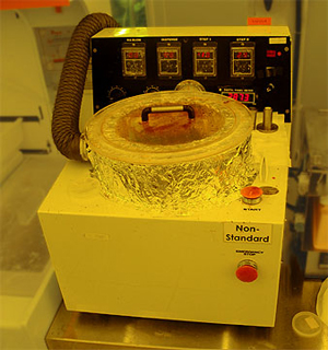
Desktop Coater
| Spin-speed range | : 0 to 5,000 rpm |
| Substrate sizes | : > 5 mm² to 4" square |
Text Area
Left Column
Image
Image
Right Column
Text Area
Solitec Coater #1
| Spin-speed range | : 250 – 5000 rpm |
| Spin-speed acceleration | : 1000 – 4000 rpm/sec |
| Substrate sizes | : Larger than 5 mm, 2 to 4", 5" square for single-side coating or 4" for double-side coating |
Text Area
Left Column
Image
Image
Right Column
Text Area
Laurell PDMS Coater
| Spin-speed range | : 0- 6000 rpm |
| Spin-speed acceleration | : 0-30000 rpm/s |
| Substrate sizes | : 2" or 4" |
Text Area
Left Column
Image
Image
Right Column
Text Area
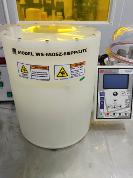
Kurabo PDMS Mixer/Deaerator
| Max. processing quantity | : 310 g x 1 container |
| Revolution | : 200 - 2000 rpm (Mixing mode) 400 -2200 rpm (Deaerate mode) |
| Rotation | : Max 800 rpm (Mixing mode) Max 66 rpm (Deaerate mode) |
| Setting time | : 0 – 30 mins x 9 steps |
Text Area
Text Area
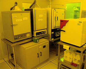
Hot Plates and Oven
Left Column
Image
Image
Right Column
Text Area
Hot Plates
Computer temperature-controller with digital readout
| Substrate sizes | : up to 6" |
| Temperature | : 50 to 250 ℃ |
| Temperature uniformity | : ± 1 ℃ |
Text Area
Left Column
Image
Image
Right Column
Text Area
High-Temperature Conventional Oven
| High-temperature oven | : Up to 450 ℃ |
| Conventional oven temperature | : Up to 250 ℃ |
| Substrate sizes | : Up to 6" |
Text Area
Left Column
Image
Image
Right Column
Text Area
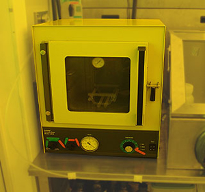
Vacuum Oven
| Temperature | : Up to 300 ℃ |
| Substrate sizes | : 1 cm² to 4" |
| Vacuum | : 0 to 30 in.Hg |
| Others | : N2 purge |
Text Area
Left Column
Image
Image
Right Column
Text Area
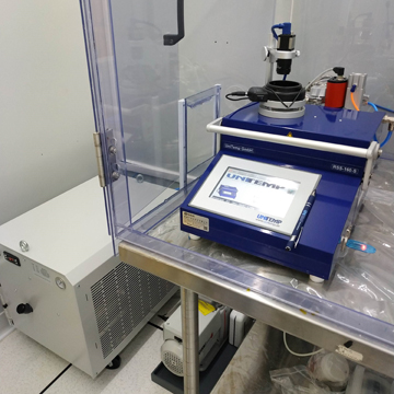
Unitemp Reflow Oven
Reflow Soldering (with Formic Acid Option)
| Substrate size | : Fragments to 160 mm |
| Substrate Thickness | : Up to 10 mm |
| Vacuum Range | : Atmosphere to 10-3 hPa or mbar |
| Oven Temperature | : Ambient to 350℃ |
| Ramp Up Rate | : Up to 120 K/min |
| Gas Flow Control | : Nitrogen at max. 5 normal litre per min |
Text Area
Text Area
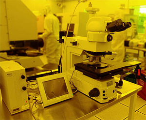
Microscope
Left Column
Image
Image
Right Column
Text Area
Nikon IC Inspection Microscope with a Digital Camera
| Contrast methods | : BF /DF/ DIC/ Fluorescence |
| Magnification | : 50× - 1500× |
| Wafer holder | : up to 6" |
| Mask holder | : 5" square |
| Digital camera | : 5M-pixel CCD |
| Display | : 8.4" TFT LCD XGA |
| Software | : Dimension measurement tool |